
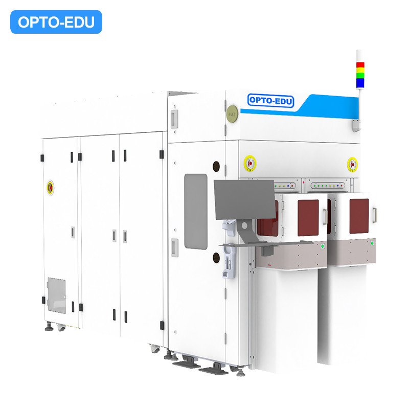
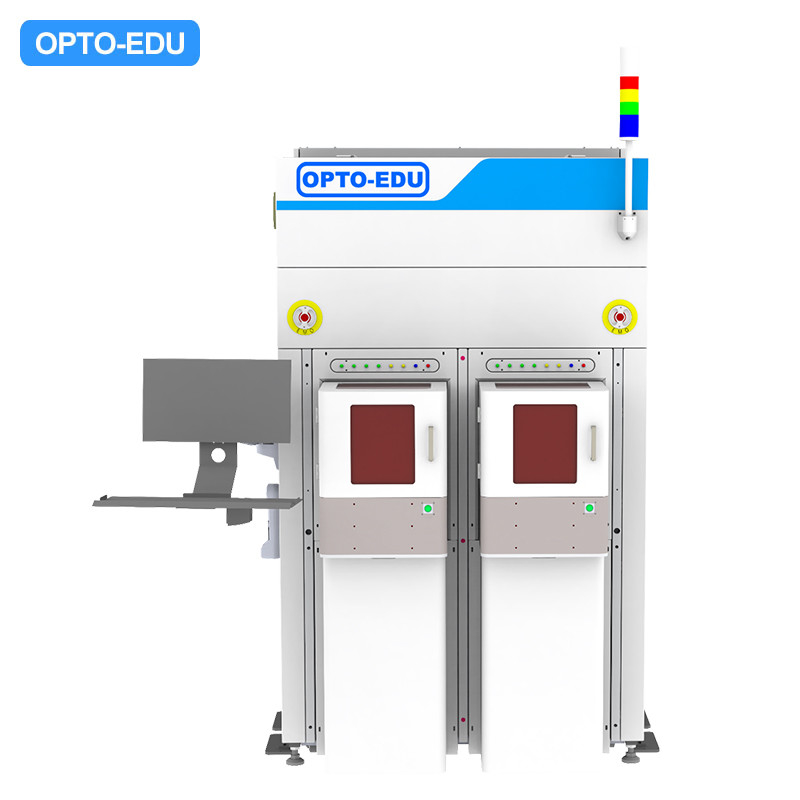
OPTO-EDU A63.7190 Microscópio Eletrônico de Varredura de Dimensão Crítica 300000x
-
Tamanho da bolachaA63.7190-68: 6/8 Polegadas
-
Resolução2.5nm (Acc=800V)
-
Voltagens de aceleração0.5-1.6KV
-
RepetitividadeEstática e dinâmica ± 1% ou 3 nm ((3 Sigma)
-
Corrente do feixe de sonda3 ~ 30 pA
-
Faixa de mediçãoFOV 0,1-2,0 μm
-
Lugar de origemChina
-
MarcaCNOEC, OPTO-EDU
-
CertificaçãoCE, Rohs
-
Número do modeloA63.7190
-
Documento
-
Quantidade de ordem mínima1 por cento
-
PreçoFOB $1~1000, Depend on Order Quantity
-
Detalhes da embalagemEmbalagem da caixa, para o transporte da exportação
-
Tempo de entrega5 a 20 dias
-
Termos de pagamentoT/T, West Union, Paypal
-
Habilidade da fontemês de 5000 PCes
OPTO-EDU A63.7190 Microscópio Eletrônico de Varredura de Dimensão Crítica 300000x
|
Um microscópio eletrônico de varredura de dimensão crítica (CD-SEM) é um SEM especializado usado para medir as dimensões de pequenas características em wafers de semicondutores, fotomascas e outros materiais.Estas medições são cruciais para garantir a precisão e a precisão dos dispositivos electrónicos fabricados.
- Não.Compatível com Wafers de 6/8 de polegada Tamanho, Magnificação 1000x-300000x - Não.Resolução 2,5 nm (Acc=800V), Tensões de Aceleração 500V-1600V - Não.Repetitividade estática e dinâmica ± 1% ou 3nm ((3 Sigma), corrente de feixe de sonda 3 ~ 30pA - Não.Projeto de sistema de transferência de wafer de alta velocidade adequado para chips de semicondutores de 3a geração - Não.Sistemas avançados de electrónica óptica e processamento de imagem, incluindo chiller, bomba seca |
|
▶Características fundamentais Os CD-SEM utilizam um feixe de elétrons de baixa energia e têm uma calibração de ampliação melhorada para garantir medições precisas e repetíveis.e ângulos das paredes laterais dos padrões. |
|
▶Objetivo Os CD-SEM são essenciais para a metrologia na indústria de semicondutores, ajudando a medir as dimensões críticas (CDs) dos padrões criados durante os processos de litografia e gravação.Os CDs referem-se aos menores tamanhos de características que podem ser fabricados e medidos de forma confiável em uma bolacha. |
|
▶Aplicações Esses instrumentos são usados nas linhas de fabricação de dispositivos eletrônicos para garantir a precisão dimensional das várias camadas e características que compõem um chip.Também desempenham um papel crucial no desenvolvimento e controlo dos processos, ajudando a identificar e corrigir quaisquer problemas que possam surgir durante o processo de fabrico.
▶Importância Sem CD-SEM, a microeletrônica moderna teria dificuldade em alcançar o alto nível de precisão e desempenho exigido pela indústria.São indispensáveis para garantir a fiabilidade e a funcionalidade dos dispositivos electrónicos modernos. |
|
▶Mudanças tecnológicas À medida que as técnicas de litografia avançam e os tamanhos das peças continuam a diminuir, os CD-SEM estão em constante evolução para atender às demandas da indústria.Novas tecnologias e avanços no CD-SEM estão a ser desenvolvidos para enfrentar os desafios da medição de padrões cada vez mais complexos |
| A63.7190 Microscópio eletrônico de digitalização de dimensão crítica (CDSEM) | ||
| Tamanho da bolacha | A63.7190-68: 6/8 polegadas | A63.7190-1212 polegadas. |
| Resolução | 2.5nm (Acc=800V) | 1.8nm (Acc-800V) |
| Voltagens de aceleração | 0.5-1.6KV | 0.3-2.0KV |
| Repetitividade | Estática e dinâmica ± 1% ou 3 nm ((3 Sigma) | Estática e dinâmica ± 1% ou 0,3 nm ((3 Sigma) |
| Corrente do feixe de sonda | 3 ~ 30 pA | 3 ~ 40 pA |
| Faixa de medição | FOV 0,1-2,0 μm | FOV 0,05 a 2,0 μm |
| Propagação | > 20 wafers/hora, | > 36 wafers/hora, |
| 1 ponto/ficha, | 1 ponto/ficha, | |
| 20 Chips/Wafer | 20 Chips/Wafer | |
| Magnificação | 1Kx~300Kx | 1Kx-500Kx |
| Precisão do estágio | 0.5 μm | |
| Fonte de elétrons | Emitente de campo térmico Schottky | |
| Comparação dos principais modelos CDSEM no mercado | |||||
| Especificações | Hitachi | Hitachi | Hitachi | Opto-Edu | Opto-Edu |
| S8840 | S9380 | S9380 II | A63.7190-68 | A63.7190-12 | |
| 1. Tamanho da bolacha | 6 polegadas/8 polegadas | 8 polegadas/12 polegadas | 8 polegadas/12 polegadas | 6 polegadas/8 polegadas | 12 polegadas. |
| 2Resolução | 5 nm (Acc=800V) | 2 nm (Acc=800V) | 2 nm (Acc=800V) | 2.5nm (Acc=800V) | 1.8nm (Acc=800V) |
| 3Tensão de aceleração. | 500-1300 V | 300-1600 V | 300-1600 V | 500-1600 V | 300-2000V |
| 4Repetitividade (estática e dinâmica) | ± 1% ou 5 nm ((3 sigma) | ± 1% ou 2 nm ((3 sigma) | ± 1% ou 2 nm ((3 sigma) | ± 1% ou 3 nm ((3 sigma) | ± 1% ou 0,3 nm ((3 sigma) |
| 5. Intervalo Ip (corrente da sonda) | 1 a 16 pA | 3-50 pA | 3-50 pA | 3-30 pA | 3-40 pA |
| 6. Tamanho do FOV | - | 50 nm-2um | 0.05-2um | 0.1-2um | 0.05-2um |
| 7.Throughput | 26 wafers/hora, | 24 wafers/hora, | 24 wafers/hora, | > 20 wafers/hora, | 36 wafers/hora, |
| 1 ponto por ficha, | 1 ponto por ficha, | 1 ponto por ficha, | 1 ponto por ficha, | 1 ponto por ficha, | |
| 5 fichas/wafer | 20 fichas/wafer | 20 fichas/wafer | 20 fichas/wafer | 20 fichas/wafer | |
Nossos produtos são vendidos em todo o mundo. Você pode ter certeza de todo o processo de nossos produtos.